Power Management Introduction
Introduction
This article is the first in a series of articles that will help the user
to get familiar with power management components. The guide provides an introduction
to different power management topologies, highlights the key selection criteria,
and provides the on-line product parametric search and design support tools
to help speed up the component selection of power management designs.
1. The basics of power conversion in applications
Selecting a power management component depends a lot on the input and output
conditions of the application.
Is the input AC or DC? Is input voltage higher
or lower than required output voltage? What is the load current? Maybe the load
is sensitive to noise, or requires a constant current (for LEDs), or maybe it
has a dynamically changing current?
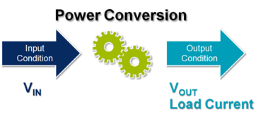
Based on the specific application requirements, different power conversion
components could be selected.
Below picture shows several examples of applications
with their typical power conversion components, all if which can be found in
Richtek’ portfolio.
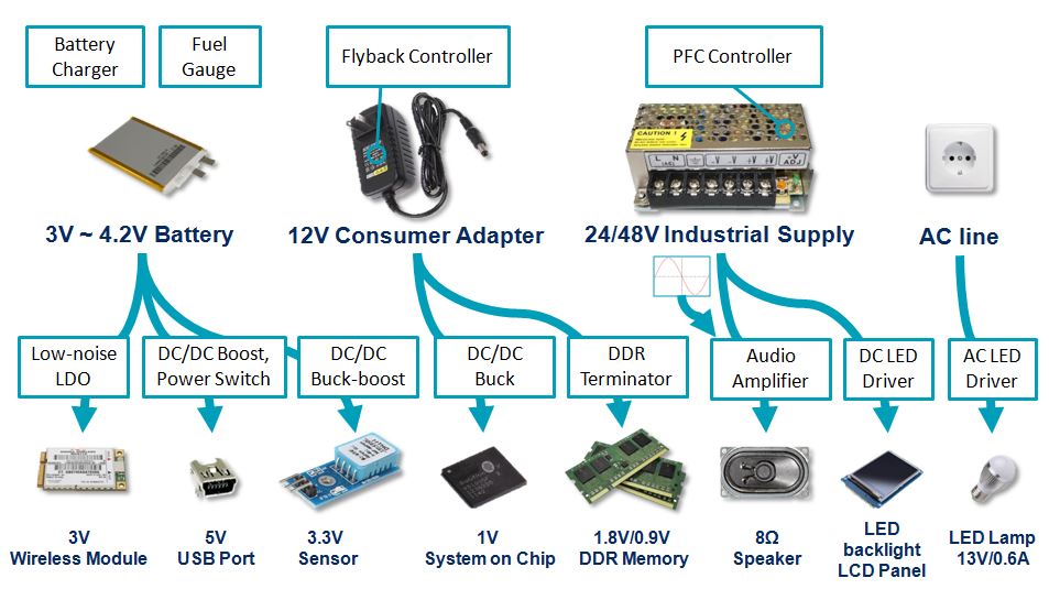
Figure 1. Example applications in power management
It is clear from the above examples that various parameters need to be considered
for optimal component choice.
The following section describes these parameters
in more detail.
2. Power management IC selection criteria
Richtek has a large portfolio of LDOs (linear regulator) and DC/DC converters/controllers.
The table below shows a quick view on general selection criteria for LDO and
DC/DC switching converter products.
The first step of design considerations is the input to output voltage difference.
(VIN - VOUT).
Specific application requirements like
efficiency, thermal limits, noise, complexity and cost need to be taken into
consideration in order to select an optimal power solution.
Table 1: Basic criteria for selecting LDO, Buck, Boost
or Buck-Boost
|
Condition
|
Topology
|
Advantage
|
Disadvantage
|
When to use
|
|
VOUT < VIN
|
LDO
(Linear Regulator)
|
·Simple
·Cheap
·Low noise
·Fast
|
·Low efficiency
·Thermal limit
|
·Low current
·Low VIN → VOUT ratio
·Noise sensitive application
|
|
Buck
|
·High efficiency
·Flexible
|
·Switch noise
|
·High current
·High VIN → VOUT ratio
|
|
VOUT > VIN
|
Boost
|
·Good efficiency
|
·Switch noise
|
·When VOUT > VIN
|
|
VOUT < > VIN
(changing VIN)
|
Buck-Boost
|
·Good efficiency
|
·Switch noise
|
·When VIN can be smaller or larger than VOUT
·i.e.: Battery input
|
3. A quick view on some key topologies and power management
components
When VOUT is smaller than VIN, the application output
current and VIN / VOUT ratio are critical criteria for
choosing an
LDO or a
Buck.
The Low drop out linear regulator or LDO is suitable for applications which
require low noise, low current and low VIN / VOUT ratio.
The basic circuit is shown in figure 2.
LDOs regulate the output voltage
by controlling the conduction of the pass element in a linear fashion. This
linear regulation provides accurate, noise free output voltage which can quickly
respond to load changes on the output. But the linear regulation also means
that the voltage difference between input and output times the average load
current is dissipated in the LDO pass element. Pd = (VIN - VOUT)
* ILOAD , so high VIN / VOUT ratios with high
load currents would lead to excessive dissipation.
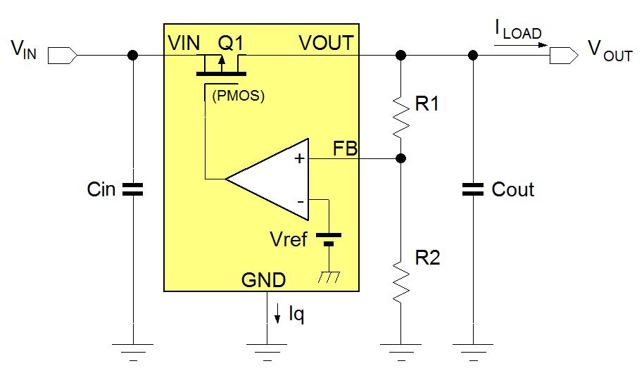
Figure 2. Basic LDO schematic
Higher power dissipation requires LDOs in larger packages, which increases
cost, PCB space and application heat. When LDO power dissipation exceeds ~ 0.8W,
it is wise to look for alternatives like Buck converters.
When selecting
an LDO, one should consider the input and output voltage range, the LDO current
capability and package dissipation capability. LDO dropout voltage is the minimum
VIN - VOUT voltage where the device can regulate. In micro
power applications, (i.e. applications that need to run from a battery for several
years) the LDO quiescent current IQ needs to be low to avoid unwanted
battery drain. These applications need special
low IQ LDOs.
Buck converters are switch-mode step-down converters which can provide high
efficiency and high flexibility at higher VIN / VOUT ratios
and higher load current. The basic circuit is shown in figure 3. Most Buck converters
contain an internal high side MOSFET and low side synchronous rectifier MOSFET,
which are in turn switched on and off via internal duty-cycle control circuit
to regulate the average output voltage. The switching waveform is filtered via
an external LC filter stage.
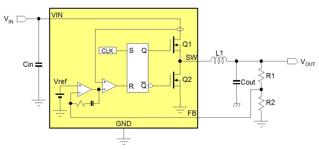
Figure 3. Basic Buck converter circuit
Due to the fact that the MOSFETs are either ON or OFF, they dissipate very
little power, and the duty-cycle control makes large VIN / VOUT
ratios possible. The internal MOSFETs Rdson mainly determines the current handling
capabilities of the Buck converter, and the MOSFET voltage ratings determine
the maximum input voltage. The switching frequency together with the external
LC filter components will determine the ripple voltage on the output. Higher
switching frequency buck converters can use smaller filter components, but switch
losses will increase. Buck converters with Pulse Skipping Mode (PSM) will reduce
their switching frequency at light load, thereby increasing light load efficiency,
which can be important in applications with low power standby modes. Special
Buck topologies like ACOT®; have very fast loop response and are very suitable for applications
that exhibit very fast load transients, like DDR, Core SoC, FPGA and ASIC supplies.
Boost converters are used when VOUT needs to be higher than VIN
. The basic circuit is shown in figure 4.
Boost converters will step-up the input voltage to a higher output voltage.
This is accomplished by charging an inductor via an internal MOSFET switch,
and discharging the inductor via a rectifier to the load when the MOSFET switch
is off. The transition from inductor charge to discharge will reverse the voltage
across the inductor, thereby stepping up the voltage higher than VIN.
The on/off duty-cycle of the MOSFET switch will determine the VOUT
/ VIN boost ratio, and the feedback loop will control the duty-cycle
to maintain stable output voltage. The output capacitor is the buffer element
to reduce the output voltage ripple.
The current rating of the MOSFET switch
together with step-up ratio will determine the maximum load current, and the
MOSFET voltage rating will determine the maximum output voltage capability.
In some boost converters, the rectifier is integrated as a MOSFET to provide
synchronous rectification.
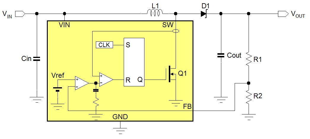
Figure 4. Basic Boost converter schematic
A Buck-Boost converter is used in applications where input voltage can vary,
either below or above the output voltage.
In the Buck-Boost converter as
shown in figure 5, the four internal MOSFET switches will be automatically configured
to form a buck when VIN exceeds VOUT and change to Boost
operation when VIN falls below VOUT. This makes Buck-Boost
ideal for battery-powered applications to extend battery life when the battery
voltage falls below the regulated output voltage value. Due to the fully synchronous
operation, the efficiency of the 4-switch Buck-Boost converter is very good.
The output current capability in Buck mode is higher than in Boost mode,
due to step-up requiring higher switch current at the same load conditions when
compared to Buck mode.
The MOSFET voltage ratings will determine the maximum
input and output voltage range.
In applications where the output voltage
does not need to be referenced to ground (like LED drivers), buck-boost converters
with a single switch and rectifier can be used. In most cases, the output voltage
is then referenced to VIN.
Many other power management components use one of the four topologies: LDO,
BUCK, BOOST or BUCK-BOOST.
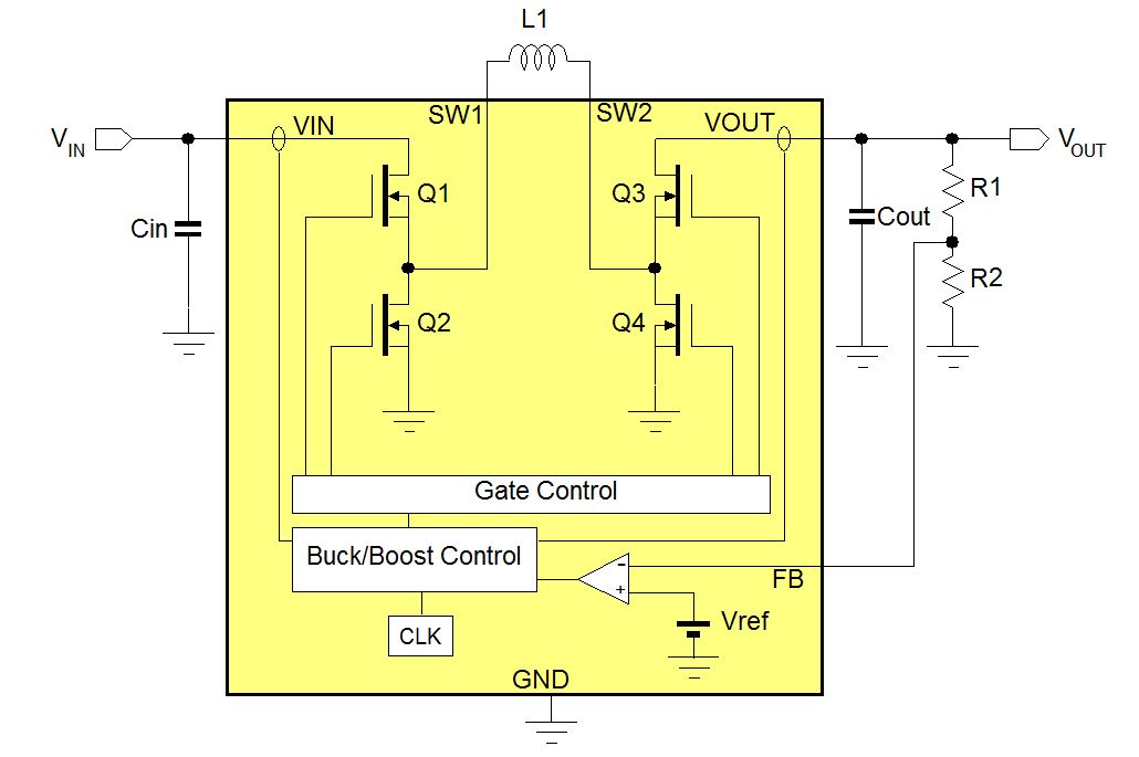
Figure 5. A Buck-boost converter with 4 internal switches
Internal or external MOSFETs?
Applications that require very large switch currents (i.e. > 10A) will
most likely use external switching MOSFETs in combination with a
buck controller or
boost controller. These configurations are often used in power converters
with output powers larger than 25W.
Buck applications with output currents >
25A will use
Multi-Phase Buck controllers to share the current over different phases.
Circuits that have very high switching voltage, for example applications
that are powered from the AC line voltage, will normally use controllers with
external high voltage MOSFETs. (For example
flyback controllers and
PFC controllers)
LED drivers will regulate for constant output current instead of constant
output voltage, because LEDs need to be driven with certain current for specific
light output. Most high brightness LEDs have a forward voltage between 3 ~ 3.5V.
Depending on the input voltage and the number of LEDs used in the LED string,
the converter can be a buck, boost or buck-boost (for example when the application
needs to cater for different LED strings).
When driving high numbers of
LEDs like in
LCD backlighting systems, multi-string LED drivers are used.
In some
off-line LED drivers,
linear LED driver topology is used.
Most LED drivers will also include
dimming functions, to be able to control the output current, thereby controlling
the LED light output.
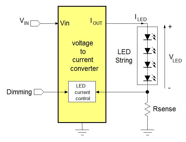
Figure 6. Basic LED driver
Key parameters for selecting LED drivers are input voltage, LED string voltage
and LED string current, single / multi-string LEDs and dimming. In
LED drivers powered from the AC line, it is also important to know whether
the application needs to be isolated or non-isolated, and whether the LED driver
needs to fulfil power factor and THD requirements.
Protection functions
Safety and reliability are important aspects of power supplies. Most converters
will include protection features which safely shut down the supply in case of
overload or too high operating temperature.
Power switches can be used to enable and disable power rails. The basic
circuit is shown in figure 7. The EN pin is used to activate the pass element
which is usually a MOSFET with a special well construction to eliminate reverse
current flow via the body diode. A current limit circuit will open the switch
when output current exceeds the current limit threshold. The FAULT pin will
be pulled low in case any of the protection functions is activated, and can
be used to signal the system that a fault condition has been encountered. Power
switches are often used to protect USB ports, which have specific maximum current
requirements and must be short-circuit proof. The main selection criteria for
power switches is the current limit level, which can either be fixed or adjustable.
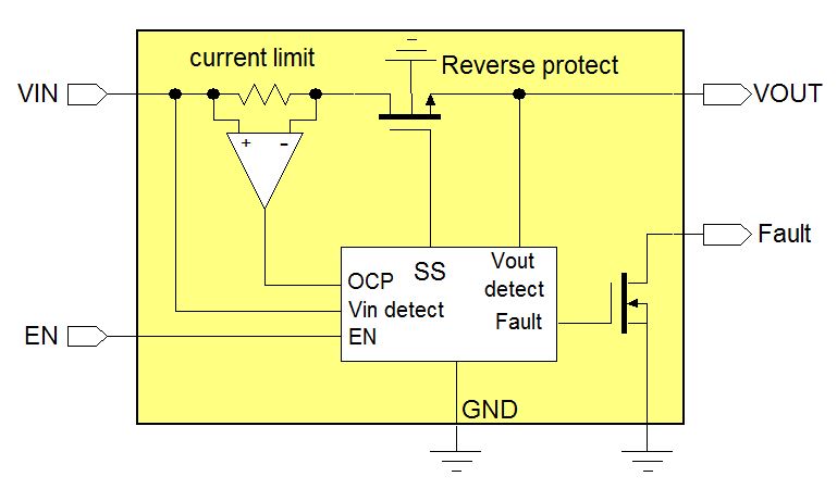
Figure 7. Power switch with various protection functions
Supply supervisor ICs will monitor a supply rail for over- or under-voltage
conditions. Figure 8 shows a typical supply supervisor that checks for supply
under-voltage conditions. When the supply rail drops below a certain level,
the IC will initiate a reset signal. This signal can then be used to reset the
MCU that is fed by the same supply rail, to avoid any data corruption that could
occur due to too low MCU supply voltage. When the supply voltage recovers to
normal levels, the supervisor IC will remove the reset signal with some delay,
to ensure correct MCU initialization.
Some supervisor ICs have a manual
reset pin as well, that can be used to reset the MCU via an external reset switch.
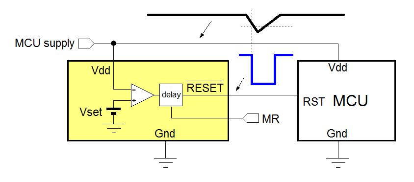
Figure 8. A supply supervisor IC that detects supply under-voltage
conditions
Selection criteria for supervisor ICs are voltage threshold, reset delay
time, open-drain or push-pull output, and options like manual reset.
Battery charger ICs can be used to provide the correct charge current and
voltage for the specific battery cell in your application. Most battery chargers
are designed for Li-Ion batteries since these most popular in hand-held equipment.
The battery charger will measure battery charge current and battery voltage,
and controls the pass MOSFET in such a way that the charge current follows the
required battery charge operation modes: pre-conditioning - constant current
- constant voltage - current cut-off. The maximum charge current can be programmed
by an external resistor, and an NTC coupled to the battery will send the battery
temperature information to the charger. Charge status pins will signal the charge
condition. Most
linear chargers for single cell Li-Ion batteries are fed by 5V supply, and
are normally used for charge currents up to 1A, for battery cells up to 1Ah.
To charge larger capacity cells, higher charge currents are needed. In this
case
switching chargers (buck topology) must be selected. Some battery chargers
contain Power Path control, which allows the system to be run from either the
adapter or the battery. Battery chargers can be selected on linear/switching
topology, single/dual input, fixed/adjustable current, with/without NTC sense,
adapter input current limit, Auto Power Path.
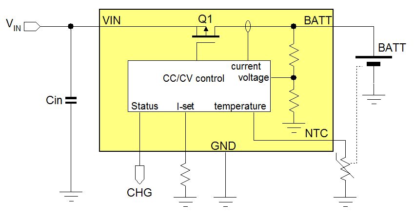
Figure 9. Basic linear battery charger circuit
AC/DC flyback controllers are used in application where a stable, isolated
supply voltage needs to be derived from the AC line voltage. Figure 10 shows
a basic flyback supply. The AC line voltage is first rectified to a high DC
voltage. The flyback supply works similar as a single switch buck-boost, where
the inductor is split to form a transformer. The flyback controller controls
the ON time of the high voltage switching MOSFET Q1, which then magnetically
energizes the transformer via a current through the primary winding. When the
switching MOSFET is OFF, the transformer energy is transferred to the secondary
winding, thereby charging the output capacitor. The transformer will also provide
the isolation between primary (hot) side and secondary (cold) side. The secondary
output voltage is sensed with a resistor network, and compared with a reference.
The regulation feedback signal is then transferred back via an opto-coupler
to the primary side controller, which adjusts the ON time of the MOSFET to maintain
a stable secondary output voltage. The flyback controller is fed from an auxiliary
winding on the transformer. Flyback supplies can be used in a wide range of
applications, from tiny charger adapters to larger main supplies up to 100W.
In applications that require low input power in standby mode, it is necessary
to reduce the switching losses of the power components. Most flyback controllers
accomplish this by switching to special burst mode operation in light load conditions.
Other important features of flyback controllers are the protection modes, EMI
reduction methods and high voltage start-up circuits for fast start-up. Flyback
controllers for lower power applications like charger adapters often make use
of Primary Side Regulation (PSR): These controllers don’t need the opto-coupler
and feedback network at secondary side; they sense the switching voltage in
the auxiliary winding, and derive the secondary output voltage from the aux
switching waveform and primary current.
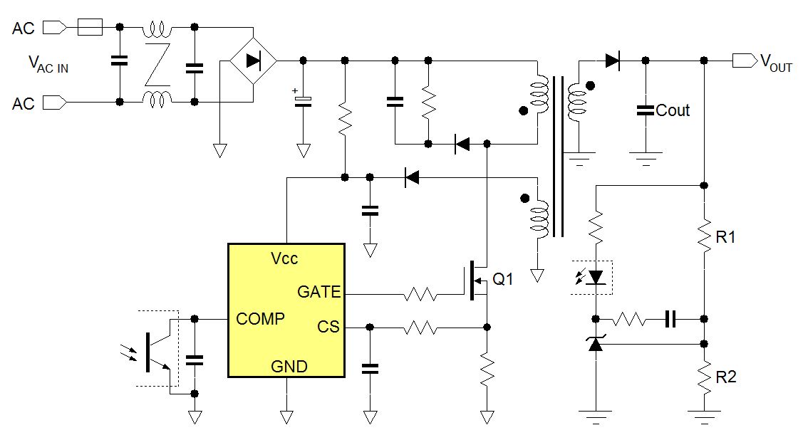
Figure 10. Basic AC/DC flyback supply
Power supplies with ratings above 75W (like open frame industrial supplies)
need to meet power factor requirements, and a PFC boost is added as a pre-conditioning
stage. The PFC boost stage will use a
PFC controller, which controls the input current to meet PF and current
harmonic requirements.
Many
isolated off-line LED drivers also make use of flyback topology, and these
LED flyback controllers use primary side sensing to control the current in the
secondary winding for accurate LED current control without the need of an opto-coupler.
AC LED lighting applications have strict requirements on Power Factor (PF) and
AC line current harmonics, so most off-line LED flyback controllers also include
functionality to achieve good power factor and low THD.